
Transistors are devices used to amplify or switch electrical signals and power. They helped revolutionise modern electrons as we know.
There are many different variations of the transistor, and two of them which are used for high power applications are the MOSFET and IGBT.
Like every other electrical and electronic component, transistors have key characteristics that determine how they function.
While both of them share many similarities, they do differ in many of these key characteristics which include;
- Switching frequency
- Voltage limits
- Current limits
- Construction
- Application
- Input impedance
- Gate control signal
These are just some of the many differences.
This article will take a closer look at MOSFETs, IGBTs and the differences between the two.
What are transistors
Since a MOSFET and IGBT are part of the transistor family, it will help to first learn a little more about the transistor.
However, if you are familiar with transistors, MOSFETs and IGBTs you can skip these sections straight to the differences part of the article.
As we just saw above, transistors are a type of semiconducting device, which in essence have the function of the humble switch.
They can be used to either conduct or insulate current or voltage.
Another neat function of a transistor is the amplification of current or voltage.
So it can function either as a switch or amplifier.
Construction of a transistor
Construction of a transistor commonly consists of placing an oppositely doped semiconductor between two similarly doped semiconductors.
They commonly consist of three terminals.
One pair of this set of three is where the control signal is applied. The control signal can either be a voltage or current.
The other pair is where the output current flows through.
Types of transistor
Transistors have two major variations;
- BJT
- FET
BJT
BJT stands for Bipolar Junction Transistor.
Its three terminals are the Base, Collector, and Emitter.
This is a current controlled transistor, which means a small current at the input allows a larger current to flow at the output.
A BJT can be further divided into two classes; PNP and NPN.
FET
FET stands for Field Effect Transistor.
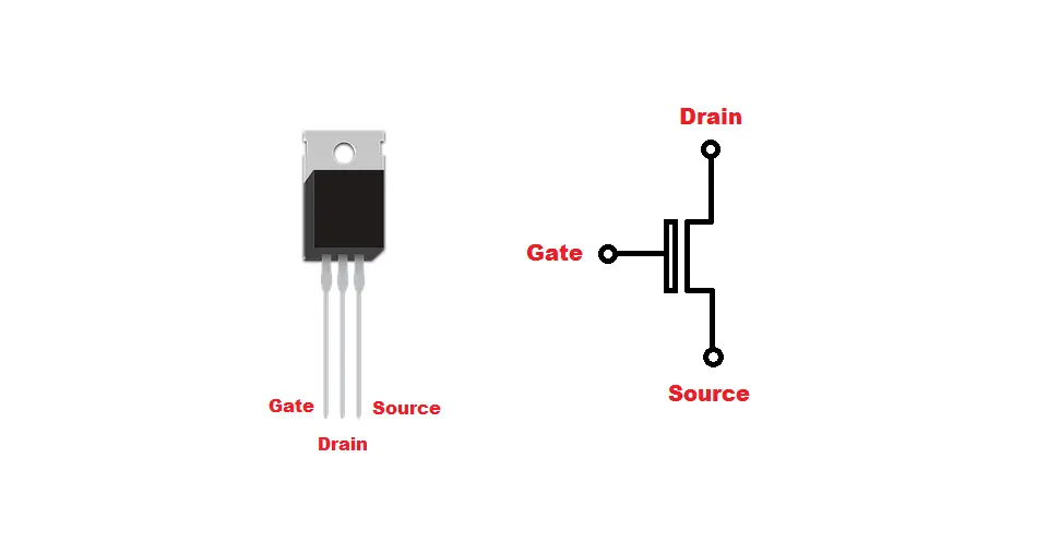
The three terminals of a FET include the Gate, Drain and Source.
This type of transistor is voltage controlled, which means a small voltage at the input allows for a larger current to flow at the output.
A FET has many variations which include;
- MOSFET
- IGBT
- JFET
- ITFFET
- FREDET
- OFET
What is a MOSFET
The first most common variation of the FET is the MOSFET which stands for Metal Oxide Semiconductor Field Effect Transistor.
MOSFETs are three terminal devices consisting of a Gate (G), Source (S) and Drain (D).
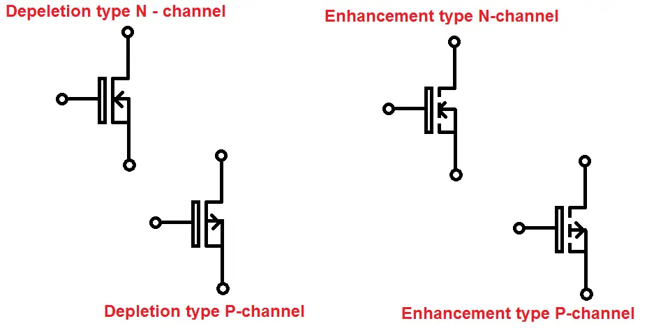
There are two main two groups of MOSFET (Enhancement and Depletion),which can either be N-Channel or P-Channel. This gives us four variations of the MOSFET which include;
- Enhancement Mode N-Channel
- Enhancement Mode P-Channel
- Depletion Mode N-Channel
- Depletion Mode P-Channel
Construction of a MOSFET
In Enhancement type MOSFETs, there is no physical connection between the source and drain, hence the broken lines in its symbol.
On the other hand, depletion MOSFETs have a small semiconducting strip that connects the source and drain terminals.
Below is an image that shows the basic construction of the MOSFET.
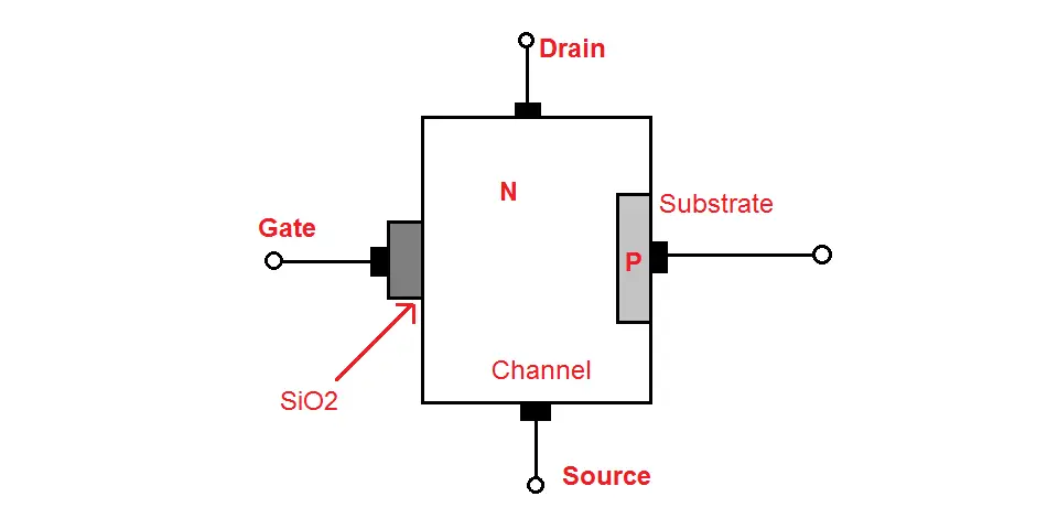
The Gate terminal is connected to a substrate where an oxide layer (SiO2) is placed. The purpose of the oxide layer is to act as an insulator.
The general construction of a MOSFET consists of a lightly doped substrate which is diffused by a heavily doped region.
The substrate used ultimately determines whether it is a P-type or N-type MOSFET.
As we saw above, MOSFETs are either Enhancement or Depletion.
N-Channel Enhancement MOSFET
The source and drain in a N-Channel Enhancement MOSFET consist of a N-type semiconductor which is heavily doped and the substrate is a P-type semiconductor.
Electrons are the main charge carriers.
P-Channel Enhancement MOSFET
On the other hand, the source and drain of P-Channel Enhancement MOSFETs are of a P-type semiconductor which is heavily doped, and the substrate is a N-type semiconductor. Holes are the major carriers here.
In enhancement mode, the source and drain are isolated.
N-Channel Depletion MOSFET
In N-channel depletion MOSFETs the source and drain are connected by a small strip of material that is a semiconductor of N-type. The substrate is a P-type semiconductor.
The main charges are electrons while the source and drain are heavily doped.
P-Channel Depletion MOSFET
The P-channel depletion MOSFET is the opposite of the N-channel, as the strip of semiconducting material connecting the source and drain is P-type. The substrate is N-type.
The main carriers are holes.
What is an IGBT
The next most common variation of a FET is the IGBT which stands for Insulated Gate Bipolar Transistor.
However, while it falls under the umbrella of a FET, the IGBT is a mashup of a MOSFET and BJT.
It combines the best parts of both these transistors to achieve high input impedance and switching speeds (of a MOSFET), as well as low voltage saturation (of a BJT).
IGBTs are aptly named because of this mashup of technologies.
They get the insulated gate technology from a MOSFET, and the output performance characteristics from a BJT.
So, you end up getting a voltage controlled transistor, with the output characteristics of a BJT.
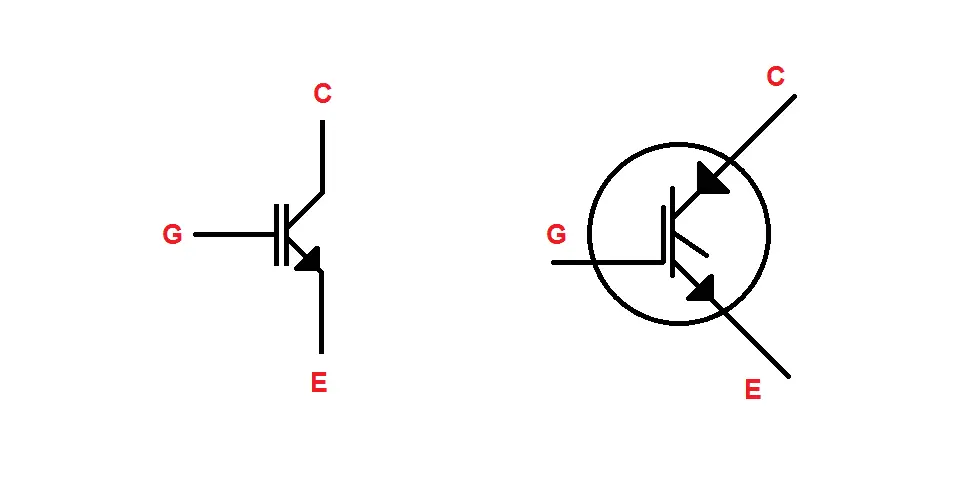
It too is a three terminal device which consists of a Gate (G), Emitter (E) and Collector (C).
Construction of IGBT
We now know that the IGBT is a combination of a MOSFET and BJT which you can see physically in the way it is constructed.
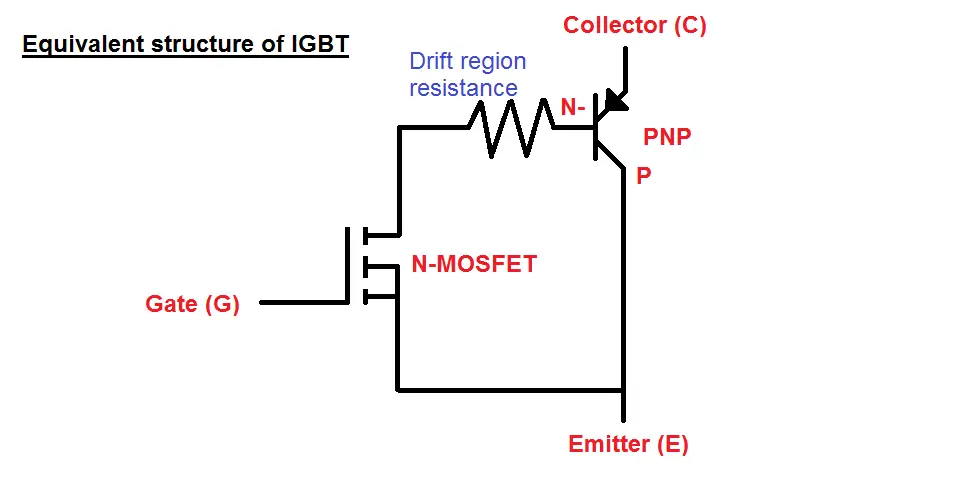
It combines an N-channel MOSFET at the input, with PNP type BJT at the output. They are connected in a Darlington configuration.
This is why the input terminal is called the Gate, and the output terminals Collector and Emitter.
Below is an image of the internal structure of an IGBT.
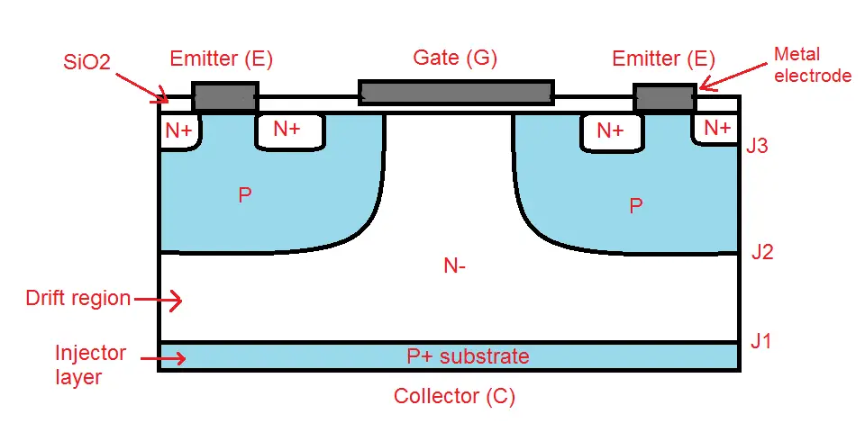
An IGBT consists of four layers of semiconducting material. This gives it a PNPN structure.
The collector terminal is fixed to the P-Layer, and the emitter is connected between the P and N layers.
MOSFET vs IGBT
So now that we have taken a closer look at a MOSFET and IGBT we can discuss the major differences between the two transistors.
While they fall under the same umbrella of transistors (FET), they do vary in many characteristics as we shall soon see.
Knowing these differences will help you decide if one is more suited for a certain application compared to another.
Let’s take a look.
MOSFET vs IGBT difference #1: Construction
Right off the bat we can see that the first major difference between the two transistors is their physical construction.
Both devices are three terminal devices, however, the IGBT combines the structures of a MOSFET and BJT which give it a set of unique qualities.
MOSFET vs IGBT difference #2: Voltage
MOSFETs and IGBTs are used in applications where they are used to isolate devices from logic circuits.
In these circuits the device in question is operating at a voltage that is higher than that of the voltage that the logic circuit is operating at.
Devices connected at the output of a MOSFET and IGBT can range in voltages from low to very high.
The amount of voltage that these devices operate at will determine how much voltage the MOSFET or IGBT will be subjected to.
So the right component will be needed for the job.
When it comes to voltages, IGBTs are best suited for high voltage applications as they can handle voltages in excess of 1000 volts.
For low voltage applications, a MOSFET is a more suitable option. They are best suited for voltages less than 250 volts.
MOSFET vs IGBT difference #3: Current
The next major difference between the MOSFET and IGBT is their current capabilities.
Another key factor when looking at devices connected to the output of transistors, is how much current they require to operate efficiently.
Just like voltage, you will need to know the maximum current that a MOSFET and IGBT will be subjected to.
As operating outside their maximum range will damage them.
Again, IGBTs are best suited for high current applications, whereas MOSFETs are a better choice for applications with low currents.
MOSFET vs IGBT difference #4: Switching frequency
If you were to close and open a mechanical switch, there is going to be a delay. You will not be able to switch between the two states instantaneously.
This is true for the switching of MOSFETs and IGBTs as well.
The time of how long it takes to switch-on and switch-off MOSFETs and IGBTs is known as switching frequency.
Switch-on times tell us the delay before current starts flowing, while switch-off times tell us the delay when current stops flowing.
MOSFETs dominate in the switching frequency department with the capability to exceed values of greater than 200kHz.
IGBTs however, have much lower switching frequency values that range less than 20kHz.
MOSFET vs IGBT difference #5: Unidirectional vs Bidirectional
When enough voltage is applied to the gate terminal of both devices, current starts to flow through their outputs (from source to drain in a MOSFET, and collector to emitter in an IGBT).
If current is only able to flow through a transistor in one direction (forward), it is considered to be a Unidirectional device.
However, if current can flow in both directions (forward and reverse), the transistor is now known as a Bidirectional device.
IGBTs only have the capability to switch current in one direction (forward), making them a unidirectional transistor.
MOSFETs can switch current in both directions (forward and reverse), making them a bidirectional transistor.
But, while the switching of current in MOSFET in the forward direction is controlled, it is uncontrolled in the reverse direction.
MOSFET vs IGBT difference #6: Power gain
Transistors are versatile devices and their unique characteristics can be utilised in many applications.
While they are primarily used as switches, transistors can also be used as an amplifier.
An amplifier has the ability to ‘amplify’ a weaker signal into a much more powerful one.
MOSFETs and IGBTs have a similar ability. A change of voltage at the input (gate) creates a huge current at their respective outputs.
So, both can amplify a weak signal into a more powerful one just like an amplifier.
One important and vital characteristic of an amplifier is its Power Gain which tells us the ratio of power at the output over the power at the input.
The higher the power gain the better, as weaker signals can be made into stronger ones.
When it comes to power gain for the MOSFET and IGBT, the IGBT wins this battle having a much higher power gain.
MOSFET vs IGBT difference #7: Conduction and Switching losses
In an ideal world, power loss would not be an issue.
However, we do not live in an ideal world so we have to deal with power loss. When it comes to MOSFETs and IGBTs, there are two major types of power losses ; conduction loss and switching loss
Conduction loss in a transistor occurs when it is conducting current, and is a product of current and voltage.
Switching loss occurs when the transistor is switching between ON and OFF states and is dependent on the duty cycle.
A MOSFET has higher conduction losses compared to the IGBT, while the IGBT has higher switching losses compared to the MOSFET.
MOSFET vs IGBT difference #8: Bipolar vs Unipolar
Earlier we saw transistors can be either unidirectional or bidirectional. The final major difference between a MOSFET and IGBT is whether it is Unipolar or Bipolar.
A bipolar transistor is a type of transistor that uses both electrons and electron holes as charge carriers, while a unipolar transistor only uses one type of charge carrier (either electron holes or electrons).
Due to its construction, an IGBT is a bipolar device using both electrons and electron holes as charge carriers.
MOSFETs are unipolar devices as they only use one type of charge carrier.
Summary of differences between a MOSFET and IGBT
If you don’t have the time to read the details of the aforementioned differences between the MOSFET and IGBT, below is a table with the summary (plus some additions).
| MOSFET | IGBT | |
| Construction | Based on the FET transistor | Hybrid of a FET and BJT transistor |
| Voltage | Low voltages (<250V) | High voltages (>1000V) |
| Current | Low current capabilities | High current capabilities |
| Switching frequency | High (>200kHz) | Low (<20kHz) |
| Unidirectional or Bidirectional | Bidirectional | Unidirectional |
| Power gain | Low | High |
| Conduction and switching loss | Conduction loss: HighSwitching loss: Low | Conduction loss: LowSwitching loss : High |
| Unipolar or Bipolar | Unipolar | Bipolar |
| Resistance to electrostatic damage | Low | Very high |
| Terminals | Gate, Source and Drain | Gate, Collector and Emitter |
Similarities between a MOSFET and IGBT
So we have just seen the major differences between the MOSFET and IGBT. But, do these transistors share any similarities?
Yes!
The most common similarity that these two transistors share is the fact that both of them are Voltage Controlled.
For a transistor to start conducting current at its output it requires a control signal at its input. This control signal can either be a current or a voltage.
If current is the parameter that controls the transistor, it is considered to be a current controlled device. But, if voltage is the controlling parameter, it is a voltage controlled device.
Since the MOSFET and IGBT both use a voltage at the input they are voltage controlled devices.
Are MOSFETs and IGBTs interchangeable?
While both transistors are used for similar applications, they do have differences as we just saw which ultimately will be a deciding factor if you can replace one with another.
Let’s take a look at some of these factors.
First is the voltage and current capability of these devices.
MOSFETs are on the lower range of voltage and current capabilities, while IGBTs have higher limits.
So, you would not be able to replace an IGBT with a MOSFET as the MOSFET won’t have the ability to handle these high voltages and currents.
On the other hand, an IGBT would be able to replace a MOSFET, but doing so is overkill. This would be analogous to cutting a slice of bread with a saw.
While possible, it probably isn’t the best idea.
A better option would be to replace multiple MOSFETs with a single IGBT.
The next factor is a parasitic body diode. This is only common with MOSFETs due to its structure. The parasitic body diode is formed between the source and drain.
This parasitic diode is made use of in many applications, especially when it comes to motor drive circuits.
If you replace a MOSFET with an IGBT in these types of circuits, you will be losing this essential parasitic body diode.
You will need to add an additional parallel diode to combat this issue.
Other factors to consider include;
- IGBT have high gate capacitance and require large current to turn on and off
- When it comes to switching applications, MOSFET can switch faster with lower loss. If you replace it with an IGBT but keep switching speeds high, you will have higher power losses.
Which is better, a MOSFET or IGBT?
So the MOSFET and IGBT aren’t entirely interchangeable.
There are many factors to consider.
But, if you had to choose, which is the better option?
Deciding on which is better really comes down to the needs of the application. It cannot be said that one is better than the other.
You have to assess the application to see what its needs are and then choose the right transistor for the job.
One transistor will be more suitable for a particular application compared to the other. But this doesn’t mean it is better overall.
For example, an IGBT is more suitable for high voltage applications compared to a MOSFET.


